
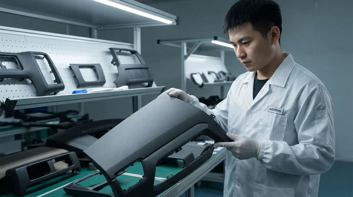
提升塑膠五金件的美觀、觸感人體工學及電磁性能,需要全面的成型後裝飾與模穴表面處理。標準的未加工塑膠成型件常顯示流痕、分模線縫或頂針痕跡,影響視覺品質。應用專業模具紋理、鑽石鏡面拋光、導電塗層或多色移印,可將裸塑膠零件轉化為可直接上市的零售組件。本技術指南回顧SPI拋光標準、VDI紋理、二次印刷方法及EMI/RFI屏蔽技術。.
目錄
SPI模具拋光(A-1鏡面)與VDI / Mold-Tech紋理
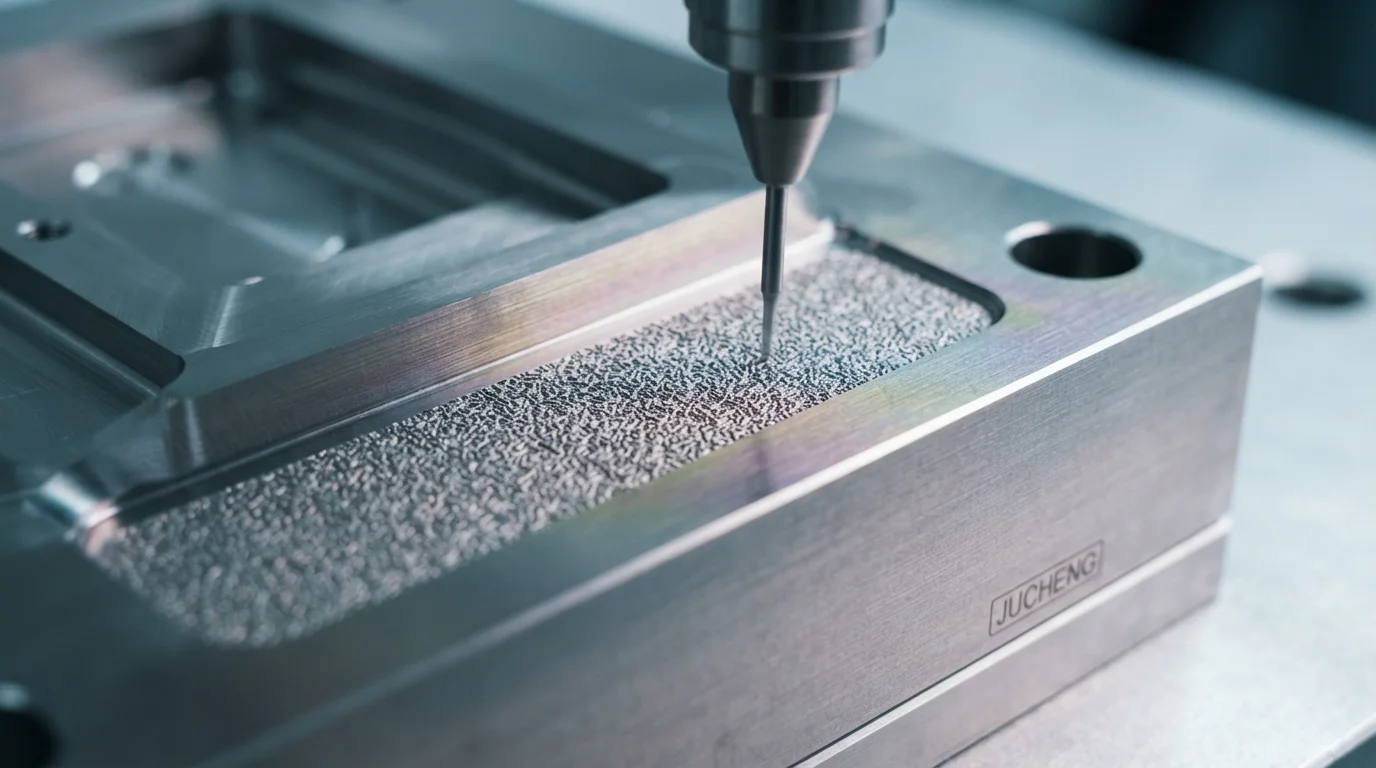
指定專業 射出成型表面處理 始於模具模穴製造階段。模穴表面準備遵循國際塑膠工業協會(SPI)拋光標準。達到 SPI A-1鏡面 需要使用鑽石膏在硬化 S136不鏽鋼, ,消除光學鏡片和高光澤 聚碳酸酯(PC) 外殼的微刮痕。應用 VDI 3400 紋理化 或 Mold-Tech 化學蝕刻 可直接在模具型腔表面賦予受控的霧面、皮革或幾何紋理。化學紋理化可遮蓋流痕和縮痕陰影,同時增強消費性電子外殼的觸感抓握力。.
模具型腔表面精加工標準包括:
- SPI A-1 鑽石拋光—以3微米鑽石拋光膏研磨硬化鋼,可形成高光澤的光學鏡面。.
- VDI 3400 放電加工紋理化—放電加工可產生從VDI 12到VDI 36的受控霧面微紋理。.
- Mold-Tech 化學蝕刻—酸蝕刻可直接在型腔鋼上形成複雜的皮革、木紋或幾何圖案。.
- 拔模角補償—Increasing vertical draft by 1° for every 0.025 mm of texture depth ensures clean part ejection without scuffing.
Secondary Ops: Pad Printing, Silk Screening, Laser Engraving & Painting
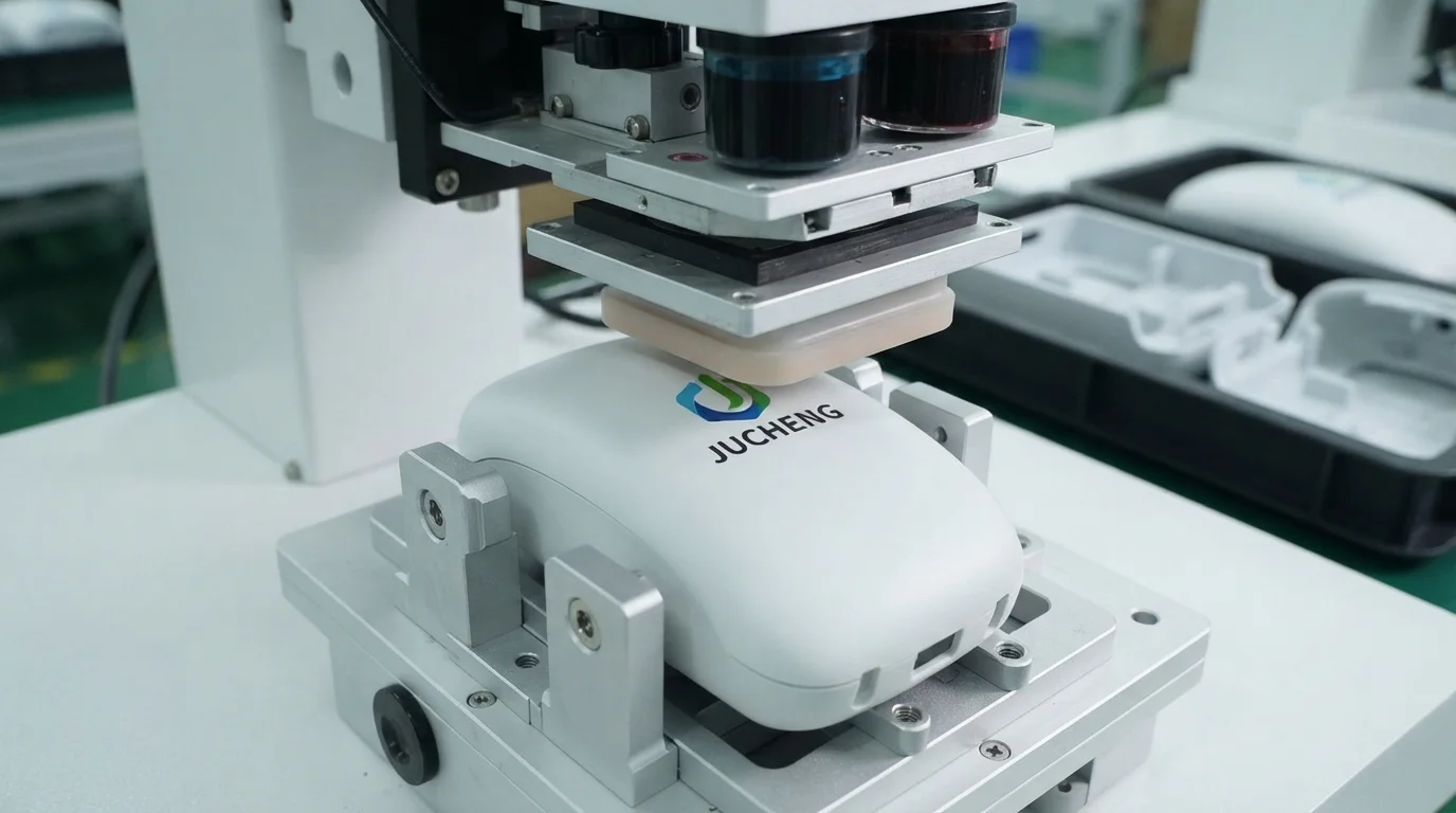
Secondary post-molding operations add functional symbols, branding logos, and protective coatings to molded ABS 或 PC/ABS parts. Utilizing multi-color pad printing transfers silicone pad ink onto complex three-dimensional curves and textured surfaces seamlessly. Laser engraving burns away superficial paint coats on backlit buttons, creating precise, light-transmitting symbols. Automated liquid spray painting and UV hard-coat applications improve scratch resistance and chemical immunity on automotive interior trims.
Conductive EMI/RFI Shielding Coatings for Electronic Enclosures
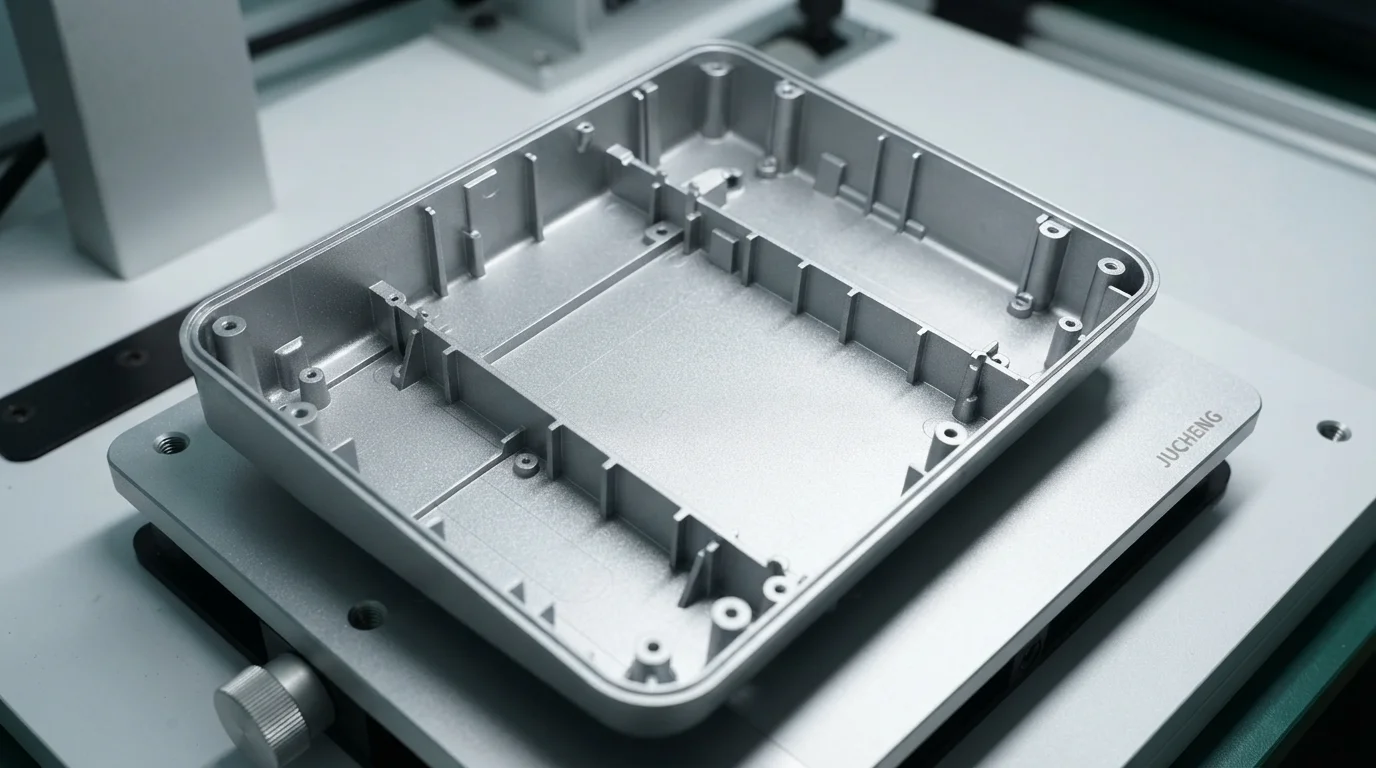
Electronic enclosures housing sensitive circuit boards require protection against electromagnetic interference. Applying conductive EMI/RFI shielding coatings inside plastic housings prevents stray radio frequency signals from disrupting internal electronics. Specialized spray painting utilizes nickel, copper, or silver conductive paint formulations to form a continuous grounding barrier. Achieving low surface resistance below 0.1 Ω/sq meets global FCC and CE electromagnetic compatibility regulations for medical and aerospace devices.
| Surface Finishing Method | Roughness / Thickness | Compatible Substrate | Primary Aesthetic / Functional Benefit |
|---|---|---|---|
| SPI A-1 Diamond Polish | Ra < 0.012 μm | PC, PMMA, Optical Resins | High-gloss transparency for optical lenses & light guides |
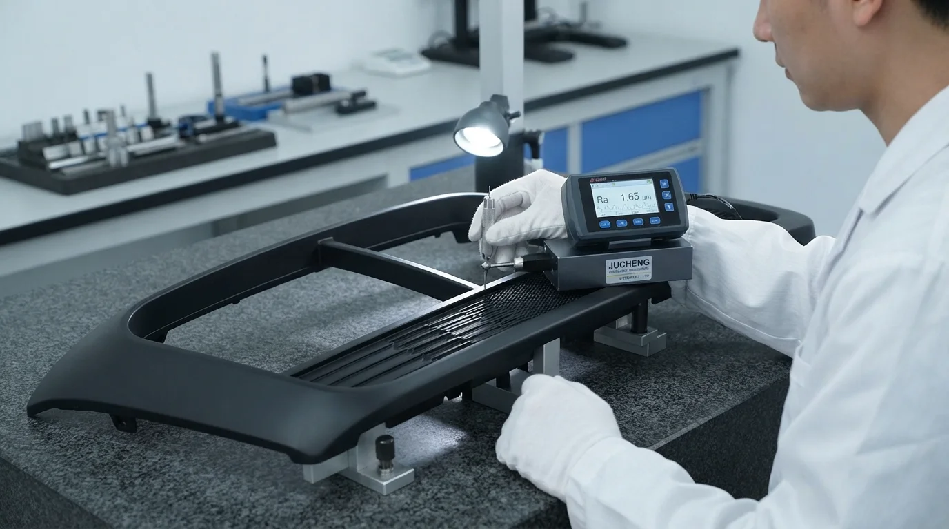
| VDI 24 Spark Texture | Ra = 1.6 μm | ABS, PC/ABS, PP, PA66 | Matte tactile finish masking sink marks & scratches |
| Conductive Nickel Coating | 25 – 50 μm dry film | ABS, PC/ABS, PBT | EMI/RFI shielding (< 0.1 Ω/sq) for electronic housings |
Frequently Asked Questions (FAQs)
What is the difference between SPI A-1 and VDI 24 surface finishes?
SPI A-1 represents an optical diamond mirror finish polished to a smooth surface roughness Ra under 0.012 microns, ideal for transparent lenses. VDI 24 is a matte spark-erosion texture produced by electrical discharge machining, offering a medium tactile grip that masks cosmetic sink marks and scratch defects on opaque enclosures.
Why do textured mold cavities require larger draft angles than polished cavities?
Textured cavity walls feature microscopic peaks and valleys that mechanically grip the shrinking plastic during cooling. Insufficient draft angles cause the plastic skin to drag against the textured steel during ejection, creating unsightly scuff marks. Adding 1° of draft for every 0.025 mm of texture depth ensures smooth release without damaging the pattern.
How do conductive spray coatings provide EMI shielding in plastic housings?
Conductive spray coatings contain microscopic nickel, copper, or silver flakes suspended in a liquid binder. When sprayed onto the internal surfaces of a plastic enclosure, the metal particles form a continuous conductive grid. This metallic layer reflects and absorbs electromagnetic radiation, preventing high-frequency noise from interfering with delicate electronic components.